Spin qubits: semiconductor quantum dots

Semiconductor spin qubits are gate-defined quantum dots in 2D (quantum well) or 1D (nanowire) semiconductor systems. Quantum information is stored in the spin degree of freedom. This kind of qubit has the advantage of taking techniques from the existing microelectronics industry for, e.g., integrating a huge number of qubits on a tiny chip or combining quantum and classial systems on the same chip.
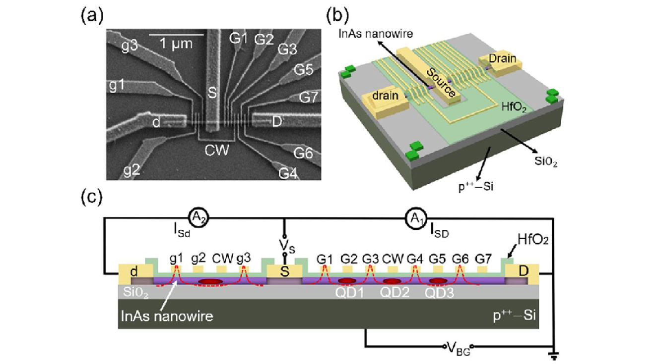
This figure from Weijie Li et al. shows three quantum dots in an InAs nanowire [QD1, QD2, and QD3 in panel (c)] and a charge sensor (also a quantum dot) coupled to the triple-dot via a coupling wire (CW)]. A quantum dot can be understood as a highly controllable artificial atom with quantized energy levels. The charge sensor is used for detecting charge states in quantum dots. While we are still working on III-V semiconductors, our next step will be moving to IV-group semiconductors which have less noise from nuclear spins.
Topological qubits: superconductor-semiconductor hybrid devices

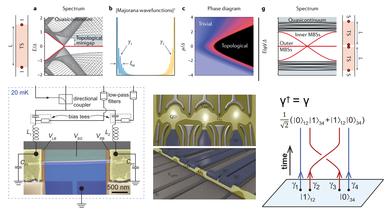
Topological qubits are very different from other solid-state qubits such as spin qubits or superconducting qubits. First, the information is stored in degenerated states (a zero-energy manifold), instead of a two-level system. Second, the logical operation is performed by exchanging positions of zero-energy quasi-particles, an operation called "braiding" (last panel in the figure), which is insensitive to detailed trajectories. Third, the quantum information is stored non-locally which enables the physical fault tolerance! Yet to be realized, this kind of qubit has attracted a lot of attention from condensed matter physicists and quantum information scientists.
While several systems are proposed for topological qubits, our group focuses on the superconductor-semiconductor (super-semi) hybrid system. The first two bottom panels show examples of devices for topolgocial qubit studies. Top panels are skematic diagrams showing how a 1d system enters the "topological" regime where extotic quasi-particles, Majorana zero modes, appear.
Figures are from Nat. Rev. Phys 2, 575–594 (2020), Nature 614, 445–450 (2023), New J. Phys. 15 045020 (2013), PNAS 115 (43) 10938-10942 (2018)
Material growth: epitaxial growth of semiconductors

The first step to make a state-of-art quantum device is growing high-quality materials. We collaborate closely with celebrated material-growth groups on semiconductors and super-semi hybrid structures. Some of their members join our group to work seamlessly on next-generation quantum devices.
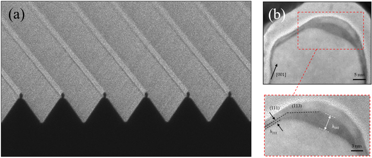
The figure shows Ge/Si core/shell nanowires on ridges of Si hills using a highly-controllable wafer-scale epitaxial growth method, from Jian-Huan Wang et al.. Ge (Si) is the darker (brighter) regime inside the dashed rectangle (panel b). Materials are grown by molecular beam epitaxy (MBE). These nanowires hold great promise for scalable quantum devices.
Condensed matter and quantum information theory

Theories inspire experiments, and vice versa. We study interactions (spin-orbital, Coulomb, exchange, et al.) inside quantum devices for better qubit fabrication, controlling, and noise canceling, as well as for our curiosity. Our theoretical activity is not limited by devices or materials in our lab. It also extends to strongly correlated systems and topological states in condensed matter physics.
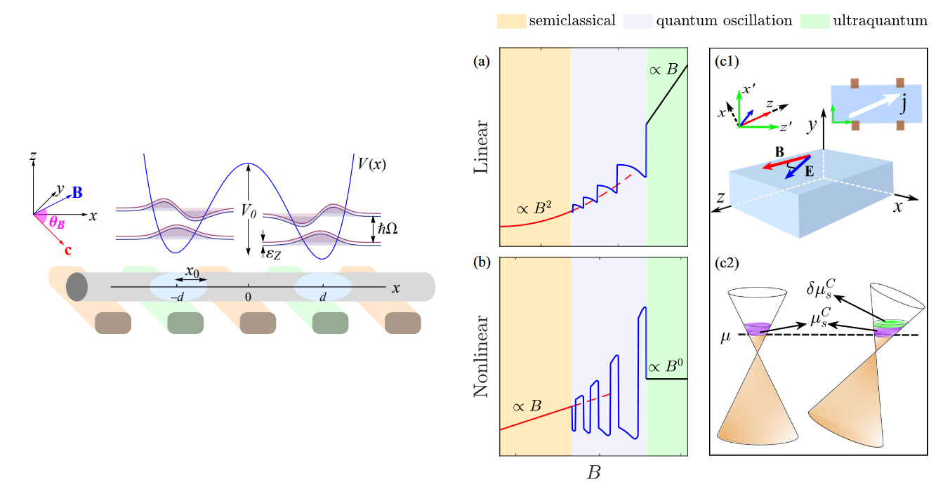
The left panel shows a schematic of two spin qubits (each is a quantum dot). Jiaan Qi et al. studied the role of spin-orbital interaction in the dynamics of the qubit pair. The right panel shows an intersting non-linear response of a Weyl semimetal in the presence of an external magnetic field, from Chuanchang Zeng et al..